- AMD’s May 21 Taiwan announcement is worth publishing because the real signal is not simply that another chip company plans to spend heavily in Asia.
- That matters because AI infrastructure is no longer constrained only by front-end silicon design.
- That is the original Grid Report angle.
- Section
- Infrastructure
- Read time
- 6 min read
- Why this page exists
- The Grid Report publishes operator-grade coverage on AI, power, infrastructure, automation, and markets.
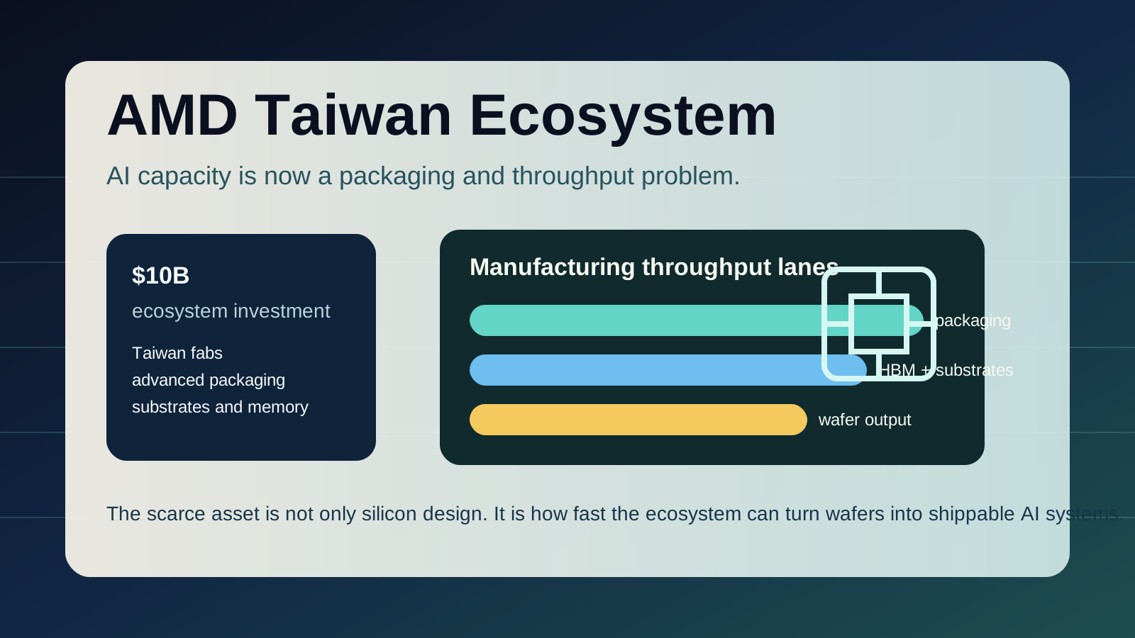
AMD’s May 21 Taiwan announcement is worth publishing because the real signal is not simply that another chip company plans to spend heavily in Asia. The stronger signal is that packaging is now being treated as a strategic throughput layer for AI infrastructure. AMD did not frame the move around generic supply-chain resilience. It framed it around scaling advanced packaging manufacturing, qualifying bridge-interconnect technology, and pushing rack-scale systems into multi-gigawatt deployment windows.
That matters because AI infrastructure is no longer constrained only by front-end silicon design. In its release, AMD said it will invest more than $10 billion across the Taiwan ecosystem to expand strategic partnerships and scale advanced packaging capabilities for AI infrastructure. It specifically called out EFB-based 2.5D packaging, panel-based interconnect work with PTI, and the supply chain required to move its Helios rack-scale platform toward high-volume manufacturing in the second half of 2026.
AMD’s signal is that the next AI hardware bottleneck may sit after chip design and before deployment, inside the packaging and interconnect lanes that turn wafers into live racks.
That is the original Grid Report angle. Advanced packaging is moving from a buried semiconductor detail into a visible deployment bottleneck. When AMD says bridge-interconnect architecture improves bandwidth and power efficiency while helping systems stay inside real-world power and cooling constraints, it is effectively saying the packaging layer now helps determine whether AI capacity can be delivered at rack scale on useful economics.
The Venice release published the same day sharpens the point. AMD says its 6th Gen EPYC CPU is the first high-performance computing product to ramp on TSMC 2nm, but the more useful line is what comes next: the CPU is becoming more critical for data movement, networking, storage, security, and orchestration as agentic workloads scale. In other words, the compute roadmap and the packaging roadmap are now fused. Faster chips do not matter enough if the interconnect, substrate, and system-integration layers cannot scale with them.
This clears the duplicate block against the site’s recent NVIDIA Vera piece and broader infrastructure stories. Vera was about the CPU re-entering the agent runtime path. This AMD story is about the manufacturing and packaging stack underneath deployment. It explains why the next AI capacity race is not only about model demand or accelerator launches, but about whether vendors can industrialize the layers between wafer and working rack.
It also clears the last-30-day similarity test against the Blackstone-Google TPU cloud, Modine cooling, and AI storage pieces. Those stories focused on financed compute capacity, thermal reservation, and rack power. This one is narrower and more supply-chain specific. It is about packaging throughput as a gating function for actual system delivery.
For operators and infrastructure investors, the read-through is practical. The AI buildout is increasingly limited by whichever hidden layer has not yet been scaled into volume: cooling, substations, or now packaging. If AMD is spending this aggressively to secure interconnect, substrate, and assembly capacity, then advanced packaging has crossed the line from engineering detail to strategic infrastructure input.
The reason to publish this now is that it is specific, timely, and better than a commodity semiconductor recap. AMD gave a date-stamped answer to a more useful question: where is the next AI hardware bottleneck moving? Its own capital plan suggests the answer is downstream of design, inside the packaging and manufacturing lanes that decide how quickly chips become live racks.
Sources
AMD Investor Relations, “AMD Announces More Than $10 Billion in Taiwan Ecosystem Investments to Accelerate AI Infrastructure,” published May 21, 2026: https://ir.amd.com/news-events/press-releases/detail/1286/amd-announces-more-than-10-billion-in-taiwan-ecosystem-investments-to-accelerate-ai-infrastructure
AMD Investor Relations, “AMD Announces Production Ramp of Next-Generation AMD EPYC Processor “Venice” on TSMC 2nm Process Technology,” published May 21, 2026: https://ir.amd.com/news-events/press-releases/detail/1287/amd-announces-production-ramp-of-next-generation-amd-epyc-processor-venice-on-tsmc-2nm-process-technology
Nawaz Lalani
Nawaz Lalani is the creator of The Grid Report and writes about AI infrastructure, grid power demand, automation systems, and the market signals shaping the physical AI economy. His focus is translating technical and industrial shifts into practical coverage for operators, investors, builders, and teams making real deployment decisions.
B.S. in Geology from UT Arlington. Covers AI infrastructure, energy systems, grid constraints, automation workflows, and market signals.
Stories are built from primary sources, utility and infrastructure signals, company disclosures, filings, and operator-grade context. The goal is to explain what changed, why it matters now, and what it means for builders, investors, utilities, and teams making real deployment decisions.
Follow the lane, not just the headline.
The strongest value in The Grid Report comes from following how AI, infrastructure, power, automation, and markets connect over time.